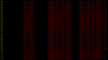
- config PAD to TTL mode:
#vi infinity2m-ssc011a-s01a-padmux-display.dtsi
- Obtain the timing table from the data sheet on the screen:

- Modify screen parameters
You can copy sdk/verify/application/jpeg2disp/src/SAT070CP50_1024x600.h and modify it on the basis:
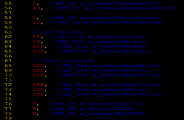
Pay attention to the values of the following variables:
m_ucPanelHSyncWidth = HSYNC.(Front Porch) + HSYNC.(Pulse Width)
m_ucPanelHSyncBackPorch = HSYNC.(Back Porch)
m_ucPanelVSyncWidth = VSYNC.(Front Porch) + VSYNC.(Pulse Width)
m_ucPanelVBackPorch = VSYNC.(Back Porch)
m_wPanelHStart = m_ucPanelHSyncWidth + m_ucPanelHSyncWidth
m_wPanelVStart = m_ucPanelVSyncWidth + m_ucPanelVBackPorch
m_wPanelWidth = HSYNC.(Display Period)
m_wPanelHeight = VSYNC.(Display Period)
m_wPanelMaxHTotal
= m_wPanelHTotal
= m_wPanelMinHTotal
= m_wPanelHStart + m_wPanelWidth
m_wPanelMaxVTotal
= m_wPanelVTotal
= m_wPanelMinVTotal
= m_wPanelVStart + m_wPanelHeight
m_dwPanelMaxDCLK
= m_dwPanelDCLK
= m_dwPanelMinDCLK
= m_wPanelHTotal * m_wPanelVTotal * FPS(自定义)
(DCLK Frequency).min <= m_dwPanelMaxDCLK <= (DCLK Frequency).max
- Modify the value of swap

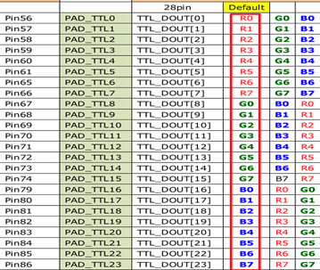
By default, the corresponding relationship between each TTL pin and RGB is as follows:
If the actual connection is not the default connection, you need to modify the swap value. Need to pay attention to the following 4 values:
m_bPanelSwapOdd_RG, when the value is 0 or 3, it corresponds to R; when the value is 1, it corresponds to B; when the value is 2, it corresponds to G;
m_bPanelSwapEven_RG, when the value is 0 or 2, it corresponds to G; when the value is 1, it corresponds to B; when the value is 3, it corresponds to R;
m_bPanelSwapOdd_GB, when the value is 0 or 1, it corresponds to B; when the value is 1, it corresponds to B; when the value is 2, it corresponds to G;
m_bPanelSwapEven_GB, when its value is 0, the RGB high and low bits are not inverted; when the value is 1, the RGB high and low bits are inverted;
When the high and low bits are not inverted, the pin correspondence is as follows:
| PAD_TTL0 | R0 |
|---|---|
| PAD_TTL1 | R1 |
| PAD_TTL2 | R2 |
| PAD_TTL3 | R3 |
| PAD_TTL4 | R4 |
| PAD_TTL5 | R5 |
| PAD_TTL6 | R6 |
| PAD_TTL7 | R7 |
After the high and low bits are reversed, the corresponding relationship between the pins becomes:
| PAD_TTL0 | R7 |
|---|---|
| PAD_TTL1 | R6 |
| PAD_TTL2 | R5 |
| PAD_TTL3 | R4 |
| PAD_TTL4 | R3 |
| PAD_TTL5 | R2 |
| PAD_TTL6 | R1 |
| PAD_TTL7 | R0 |
文档更新时间: 2020-10-24 18:15 作者:admin
